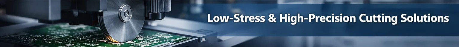
Precision Depaneling Designed to Protect PCB Integrity
As PCB designs become thinner and more complex, controlling mechanical and thermal stress during depaneling is critical. Our Low-Stress & High-Precision Cutting Solutions combine advanced routing, laser processing, and vision-guided control to deliver clean edges, accurate cuts, and reliable protection for sensitive PCB assemblies.
These solutions are engineered to minimize stress transfer, reduce the risk of micro-cracks, and ensure consistent quality across high-reliability applications.
Why Low-Stress Cutting Matters
Even minor stress introduced during depaneling can compromise PCB reliability.
Common risks include:
Micro-cracks in copper traces and solder joints
Delamination of multilayer boards
Damage to fine-pitch or fragile components
Reduced long-term reliability in high-stress environments
Low-stress cutting is essential for manufacturers focused on quality, yield, and product lifespan.
Core Technologies
Advanced Routing Control
Optimized tool paths, controlled feed rates, and precise spindle management reduce vibration and mechanical stress during cutting.
Laser Depaneling Technology
Non-contact laser cutting eliminates mechanical force, making it ideal for ultra-thin, high-density, and sensitive PCB designs.
Vision-Guided Alignment
CCD vision systems provide accurate offset correction and cutting path verification, ensuring consistent precision across every panel.
Intelligent Process Control
Software-driven parameter management allows fine adjustment of cutting speed, depth, and sequence for different board designs.
Supported Depaneling Methods
Our low-stress, high-precision solutions support multiple cutting technologies:
Router depaneling for complex outlines and controlled edge quality
Milling cutter depaneling for stable, low-vibration separation
Laser depaneling for contact-free, high-precision processing
Hybrid solutions combining mechanical and laser technologies
Each method is selected based on PCB material, thickness, and reliability requirements.
Typical Applications
These solutions are widely applied in industries demanding high precision and reliability:
Medical and high-reliability electronics
Automotive electronics and safety-critical systems
Industrial control and power electronics
Communication and networking equipment
Advanced consumer electronics
Quality Validation & Reliability
All cutting solutions are validated through real production testing. Process monitoring, tool condition management, and repeatability verification ensure consistent performance and predictable results over long production cycles.
Precision Without Compromise
If your production requires clean edges, consistent accuracy, and minimal stress on PCB assemblies, our low-stress and high-precision cutting solutions provide a proven approach.
Contact our engineering team to discuss your PCB structure and quality requirements.
Ready to Upgrade Your PCB Depaneling Process?